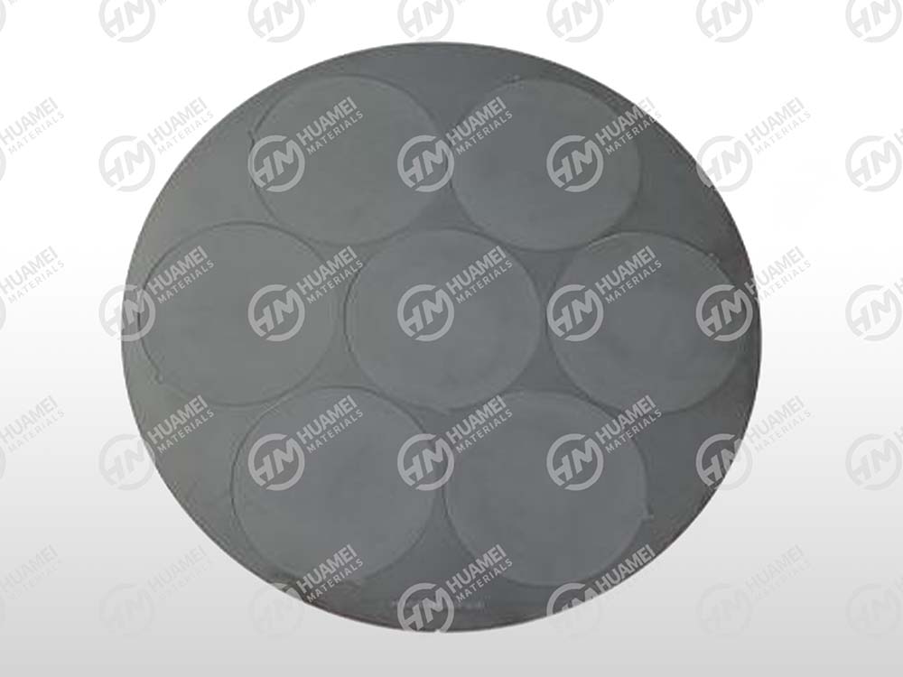
Description
Silicon carbide carriers/trays are formed and sintered at high temperatures through processes such as cold isostatic pressing, casting, or 3D printing. It is also possible to perform precision machining on the outer diameter, thickness dimensions, number and size of acupoints, position and shape of the cutting groove according to the user's design drawings to meet their specific usage requirements.
In semiconductor manufacturing processes, wafer carriers are the core consumables in high-temperature and highly corrosive environments, and their performance directly affects process yield and cost. In recent years, silicon carbide (SiC) ceramic carriers/trays have gradually replaced traditional graphite based carriers due to their unique material properties, becoming a key supporting material for the manufacturing of high brightness LEDs, compound semiconductors, and power devices.
SiC Carrier Tray is a precision structural component made of silicon carbide ceramics as its core material. With the excellent performance of silicon carbide ceramics, it plays a key role in carrying, positioning, heat transfer, and protection in high-end manufacturing fields such as semiconductors, photovoltaics, and new material preparation. It is one of the core components to ensure process stability and product yield.
Specifications
KCE® SiSiC/RBSiC/SSiC Technical Data Sheet
| Technical Parameters | Unit | SiSiC/RBSiC Value | SSiC Value |
| Silicon Carbide content | % | 85 | 99 |
| Free Silicon content | % | 15 | 0 |
| Bulk Density 20°C | g/cm³ | ≥3.02 | ≥3.10 |
| Open Porosity | Vol % | 0 | 0 |
| Hardness HK | kg/mm² | 2600 | 2800 |
| Flexural Strength 20°C | MPa | 250 | 380 |
| Flexural Strength 1200°C | MPa | 280 | 400 |
| 20 – 1000°C (Coefficient of Thermal Expansion) | 10–6 K–1 | 4.5 | 4.1 |
| Thermal Conductivity 1000°C | W/m.K | 45 | 74 |
| Static 20°C(Modulus of Elasticity ) | GPa | 330 | 420 |
| Working temperature | °C | 1300 | 1600 |
| Max. Service Temp (air) | °C | 1380 | 1680 |
Applications
Particularly suitable for precision ceramic structural components used in ICP etching processes, PVD processes, RTP processes, and CMP process carriers in the manufacturing of optoelectronic lighting epitaxial wafers.
Advantages
Excellent mechanical properties: such as high strength, high hardness, and high elastic modulus;
Resistance to plasma impact;
Good thermal conductivity, the product has excellent temperature uniformity;
Good thermal shock resistance, capable of rapid temperature rise and fall.